Home > PCB Design and Manufacturing
PCB Design and Manufacturing
Schematic Design
PCB Layout and Routing
Mechanical Engineering and Design
Comprehensive Design Evaluation
Old Design Reverse Engineering
Manufacturing Documentation Preparation
Rapid PCB Prototyping
PCB Manufacturing and Assembly
Box Builds, Cable Assemblies, and Wire Harnesses
Home > PCB Design and Manufacturing
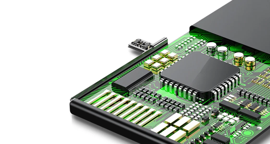
EIPEKS has been specializing in PCB development for over a decade. With our extensive expertise and resources, we fully support your projects. Whether analog or digital circuits, single-layer, double-layer, or multi-layer PCBs, we offer efficient, high-quality service from design to final production. Our main services include:
Schematic Design
PCB Layout and Routing
Mechanical Engineering and Design
Comprehensive Design Evaluation
Old Design Reverse Engineering
Manufacturing Documentation Preparation
Rapid PCB Prototyping
PCB Manufacturing and Assembly
Box Builds, Cable Assemblies, and Wire Harnesses
Standard PCB Development
The list here shows our standard PCB development capabilities, not our maximum potential. If your needs go beyond these specifications, please reach out to us.
Details of Standard PCB Development:
Materials
FR-4
370HR
Rogers
Nelco Buried Capacitance
FR406
FR408
Taconic
Polyimide
Teflon
Arlon
Hybrid FR-4 / Rogers
Layer Count
1 to 18 Layers
Minimum line spacing
0.003″
Material Thickness
0.002″ to 0.300″
Minimum Annular Ring
0.005″
Minimum drilled hole size
0.008″
Maximum board size
35″ x 46″
Maximum Copper Thickness
5oz.
Solder Mask
SMOBC, LPI or Dry Film
Finish Plating
HASL
Lead Free HASL
Immersion Silver
ENIG
ENEPIG
Matte Tin Plate
Soft / Hard Gold for Tabs and SMT
Selective Gold
Palladium
Silkscreen Colors
White
Yellow
Black
Solder Mask Colors
Green
Blue
Red
Black
Clear
Panelization
Green
Black
Panelization
Laser Vias
Tented Vias
Plated Slots
Edge Plating
Controlled Dielectrics
Conductive Filled Vias
Blind/Buried Vias
ITAR
Materials
FR-4
370HR
FR406
FR408
Nelco Buried Capacitance
Polyimide
FR408
FR408
Taconic
Taconic
Hybrid FR-4 / Rogers
Layer Count
1 to 18 Layers
Minimum line spacing
0.003″
Material Thickness
0.002″ to 0.300″
Minimum Annular Ring
0.005″
Minimum drilled hole size
0.008″
Maximum board size
35″ x 46″
Maximum Copper Thickness
5oz.
Solder Mask
SMOBC, LPI or Dry Film
Finish Plating
HASL
Lead Free HASL
Immersion Silver
ENIG
ENEPIG
Matte Tin Plate
Soft / Hard Gold for Tabs and SMT
Selective Gold
Palladium
Silkscreen Colors
White
Yellow
Black
Solder Mask Colors
Green
Blue
Red
Black
Clear
Panelization
Routing
V-Groove
Other Services
Laser Vias
Tented Vias
Plated Slots
Conductive Filled Vias
Controlled Dielectrics
Edge Plating
Blind/Buried Vias
ITAR
Common PCB Substrates
FR-4, High Temp
FR-4, High Temp
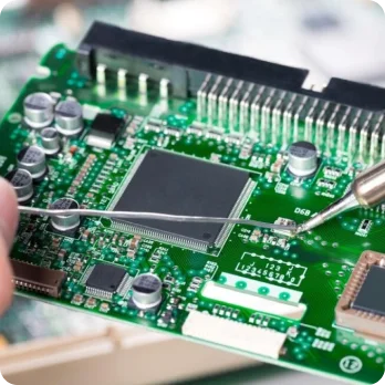
Advantages:
- High-Temperature Stability: It can operate at higher temperatures, making it suitable for high-temperature environments.
- Cost-Effective: It is more affordable compared to other high-performance substrates.
- Good Mechanical Properties: It offers high mechanical strength and toughness.
- Widely Used: It is commonly used in various electronic devices with mature technology.
Disadvantages:
- Lower Electrical Performance: Its electrical performance is lower compared to high-frequency substrates.
- Thermal Expansion: It has a high thermal expansion coefficient, which can lead to heat management issues.
- Moisture Absorption: It has high moisture absorption, which can affect electrical performance.
Rogers 3000 Series
Rogers 3000 Series
Advantages:
- Excellent Electrical Performance: Its low dielectric constant and low dielectric loss make it suitable for high-frequency applications.
- Good Thermal Stability: It maintains stable electrical performance at high temperatures.
- Low Dielectric Constant: It is suitable for high-speed signal transmission.
Disadvantages:
- Higher Cost: It is more expensive compared to FR-4.
- Processing Difficulty: It is more challenging to process and drill.
Rogers 4000 Series
Rogers 4000 Series
Advantages:
- Excellent High-Frequency Performance: Its low dielectric constant and low dielectric loss make it suitable for high-frequency and microwave applications.
- Good Thermal Stability: It performs stably in high-temperature environments.
Disadvantages:
- Higher Cost: It is more expensive compared to FR-4.
- Processing Difficulty: It is more complex to process and handle than FR-4.
Rogers 5000 Series
Rogers 5000 Series
Advantages:
- Excellent High-Frequency Performance: It provides the best dielectric properties and low loss.
- High Thermal Stability: It is suitable for extreme temperature conditions.
Disadvantages:
- High Cost: It is one of the most expensive substrates.
- Processing Difficulty: Advanced techniques are required for processing and drilling.
Teflon
Teflon
Advantages:
- Extremely Low Dielectric Constant: It is suitable for high-frequency applications.
- Excellent Chemical Resistance: It has good resistance to various chemicals.
- Low Dielectric Loss: It reduces signal loss.
Disadvantages:
- Very High Cost: It is much more expensive compared to other substrates.
- Processing Difficulty: Advanced techniques are required for processing and drilling.
TMM
TMM
Advantages:
- Excellent Thermal Conductivity: It provides efficient heat management and is suitable for power-dense applications.
- Stable Electrical Performance: It offers good electrical performance.
Disadvantages:
- High Cost: It is more expensive than traditional substrates.
- Complex Processing: It is more difficult to process.
Aluminum
Aluminum
Advantages:
- Excellent Thermal Conductivity: It effectively dissipates heat and is suitable for high-power applications.
- High Mechanical Strength: It has excellent mechanical strength.
Disadvantages:
- Poor Electrical Performance: It is not suitable for high-frequency applications.
- Higher Cost: It is more expensive than standard FR-4 substrates.
Arlon
Arlon
Advantages:
- Good High-Frequency Performance: It has a lower dielectric constant and loss factor.
- Good Thermal Stability: It can withstand higher temperatures.
Disadvantages:
- Higher Cost: It is more expensive compared to traditional FR-4.
- Processing Difficulty: It requires advanced processing techniques.
Taconic
Taconic
Advantages:
- Excellent High-Frequency Performance: It has a low dielectric constant and low dielectric loss.
- Strong Heat Resistance: It can work stably in high-temperature environments.
Disadvantages:
- Expensive Price: It has a high cost.
- Processing Difficulty: It is more complex to process and handle.
Polyamide
Polyamide
Advantages:
- High Temperature Resistance: It has excellent high-temperature performance.
- Good Mechanical Properties: It has high strength and good toughness.
Disadvantages:
- Higher Cost: It is more expensive than standard FR-4 substrates.
- Moisture Absorption: It may absorb moisture, affecting electrical performance.
PCB Development Process
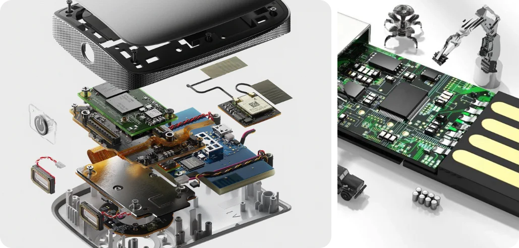
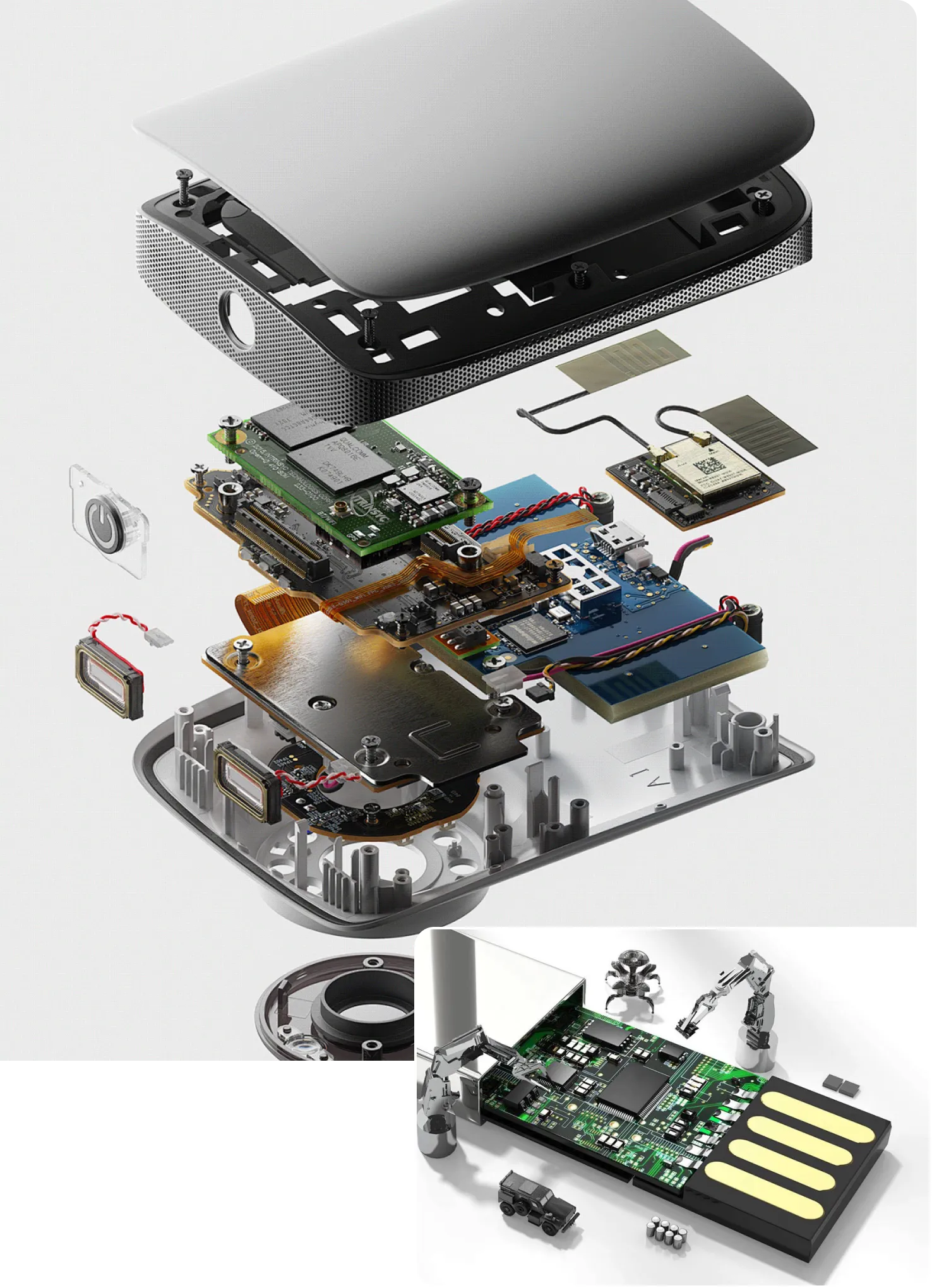
Step 1
PCB Design
01
Schematic Design
- Schematic Design
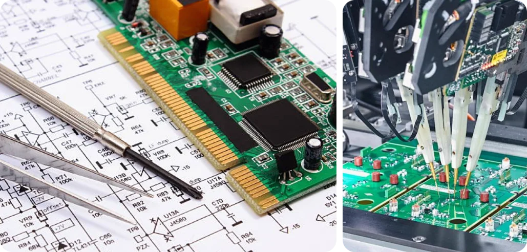
Our engineering team will carefully draw detailed CAD schematics based on your requirements, including all electronic component symbols and pad patterns, to ensure proper circuit connections. Then, we will review these schematics to verify the accuracy of layout constraints and data, ensuring that they can be correctly synchronized with the PCB layout database. Finally, we will format the schematics according to your document requirements and provide a traceable document that records all subsequent changes and revision history.
02
- PCB Layout and Routing
PCB Layout and Routing
PCB layout and routing are key steps in turning the schematic into a physical circuit board. First, our engineering team will perform the component layout and arrange the electronic components on the circuit board to optimize space utilization and signal integrity. Next, we route the connections according to the schematic, ensuring signal paths meet design requirements and avoid interference and signal loss. Finally, we use design rule checking (DRC) to verify whether the routing meets the design specifications and manufacturing standards to ensure the reliability and effectiveness of the design.
03
Mechanical Design
- PCB Layout and Routing
The mechanical design phase involves the design of the PCB shell and its integration with the overall equipment. Our mechanical engineering team designs shells, brackets, and other parts that fit the PCB. Through 3D modeling and simulation, we ensure that the design not only meets functional requirements but also optimizes heat dissipation, improves structural strength, and ensures compatibility with other components.
04
- PCB Layout and Routing
Comprehensive Design Evaluation
After the PCB design is completed, we need to conduct a series of key evaluations to ensure the quality and manufacturability. First, we review the Bill of Materials (BOM) to verify that all parts match the design and that component pricing and availability meet requirements. Next, the Design for Manufacturing (DFM) review focuses on whether the component layout and routing are suitable for manufacturing processes, ensuring smooth assembly. Then, We perform a Design for Testability (DFT) review to verify the board’s testability, including built-in test points, test fixtures, and software to ensure correct assembly. Finally, the usability review checks for problems that may cause operational difficulties, such as unclear silkscreen markings or improper component placement. All problems found and suggestions will be reported to the customer to optimize the final design and improve production and use efficiency.
05
Old Design Reverse Engineering
- PCB Layout and Routing
After the PCB design is completed, we need to conduct a series of key evaluations to ensure the quality and manufacturability. First, we review the Bill of Materials (BOM) to verify that all parts match the design and that component pricing and availability meet requirements. Next, the Design for Manufacturing (DFM) review focuses on whether the component layout and routing are suitable for manufacturing processes, ensuring smooth assembly. Then, We perform a Design for Testability (DFT) review to verify the board’s testability, including built-in test points, test fixtures, and software to ensure correct assembly. Finally, the usability review checks for problems that may cause operational difficulties, such as unclear silkscreen markings or improper component placement. All problems found and suggestions will be reported to the customer to optimize the final design and improve production and use efficiency.
Step 2
PCB Manufacturing
01
Manufacturing Documentation Preparation
- Manufacturing Documentation Preparation
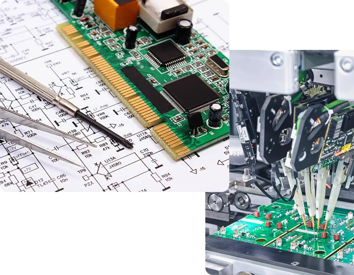
During the manufacturing documentation preparation phase, we organize and format all design files needed for production. This includes generating detailed Gerber files, drill and pad layout files, schematics, assembly drawings, Bills of Materials (BOM), etc. Our team ensures that all files are accurate and meet manufacturing standards and specifications to support a smooth production process.
02
- Rapid PCB Prototyping
Rapid PCB Prototyping
We provide rapid PCB prototyping services to verify and test design concepts in a short period of time. After completing the PCB design and circuit diagram, our engineers immediately conduct a detailed review of the Gerber files to ensure that their data is accurate and meets manufacturing standards. Once approved, we will quickly generate PCB prototypes through steps such as etching, drilling and lamination.
03
- PCB Manufacturing and Assembly
PCB Manufacturing and Assembly
In the PCB manufacturing and assembly phase, we use advanced production technology and equipment to turn design files into actual circuit boards. Our process ranges from detailed review of design documents, PCB production (including pattern transfer, etching, drilling and lamination) to component mounting, soldering and final electrical testing. Through these precise steps, we ensure that each PCB is of high quality and reliability and meets strict performance and functional requirements.
04
- Box Builds, Cable Assemblies, and Wire Harnesses
Box Builds, Cable Assemblies, and Wire Harnesses
We provide comprehensive design and manufacturing services for box builds, cable assemblies, and wire harnesses to achieve full product assembly and functional integration. Box builds include the entire device or system that is finally assembled, covering all electronic components, mechanical parts, and other related components to ensure that they can work in coordination and achieve the expected functions. Cable assemblies are composed of cables and connectors, which are responsible for connecting different electronic devices or systems. They focus on cable type, length, shielding, and connection method to ensure the reliability of signal transmission. Wire harnesses combine multiple cables and wires to simplify electrical connections, reduce clutter, and improve overall system reliability.
Application Areas

Consumer Electronics
Phone, TV, Computer, Tablet, Game Console

Military and Aerospace
Radar System, Satellite Communication Device
Industrial Control
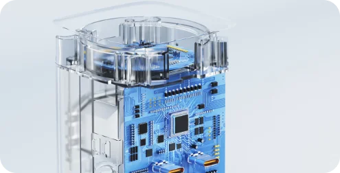
Automation Equipment, Sensor, Control Panel
Instruments and Meters
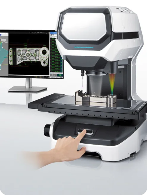
Measuring Instrument, Testing Equipment
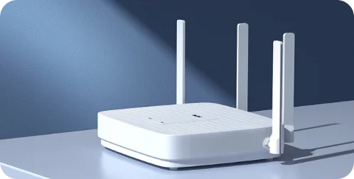
Communication Devices
Router, Switch, Wireless Base Station
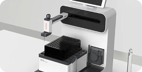
Environmental Technology
Air Quality Monitor, Water Quality Tester

Medical and Health
Wearable Device, Electronic Pill Organizer, Thermometer, Monitor

Home Appliances
Refrigerator, Washing Machine, Microwave
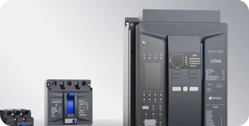
Power Systems
Power Management System, Power Supply Equipment

Consumer Electronics
Phone, TV, Computer, Tablet, Game Console
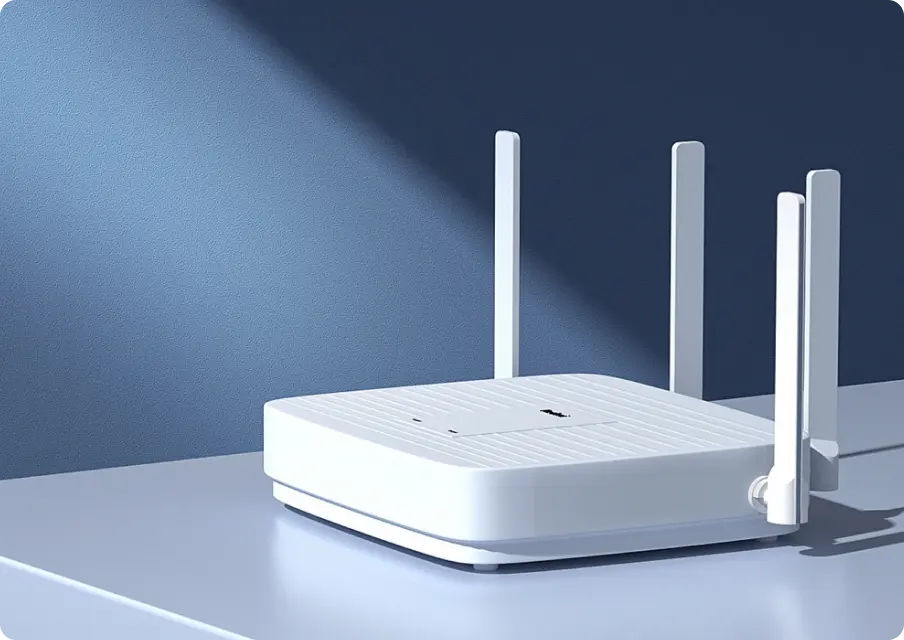
Communication Devices
Router, Switch, Wireless Base Station
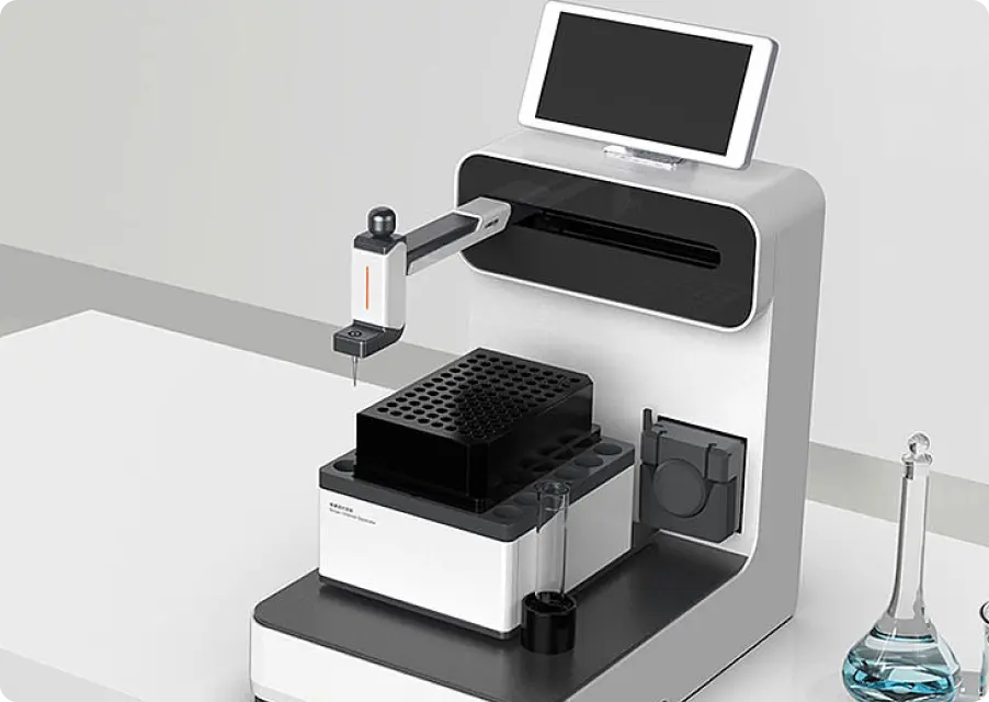
Environmental Technology
Air Quality Monitor, Water Quality Tester
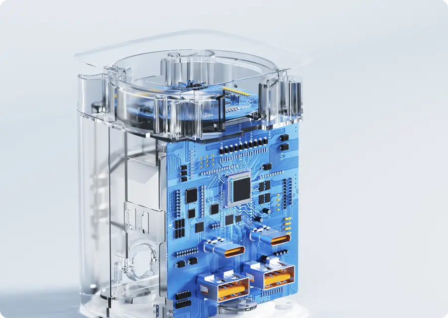
Industrial Control
Automation Equipment, Sensor, Control Panel
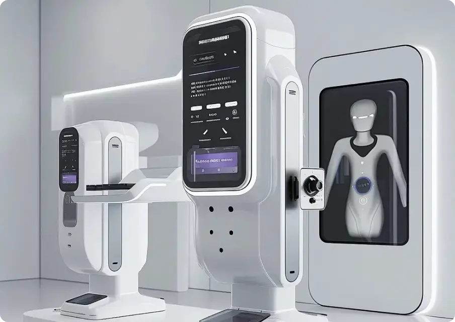
Medical and Health
Wearable Device, Electronic Pill Organizer, Thermometer, Monitor, Medical Imaging Equipment

Military and Aerospace
Radar System, Satellite Communication Device, Aircraft Control System

Home Appliances
Refrigerator, Washing Machine, Microwave
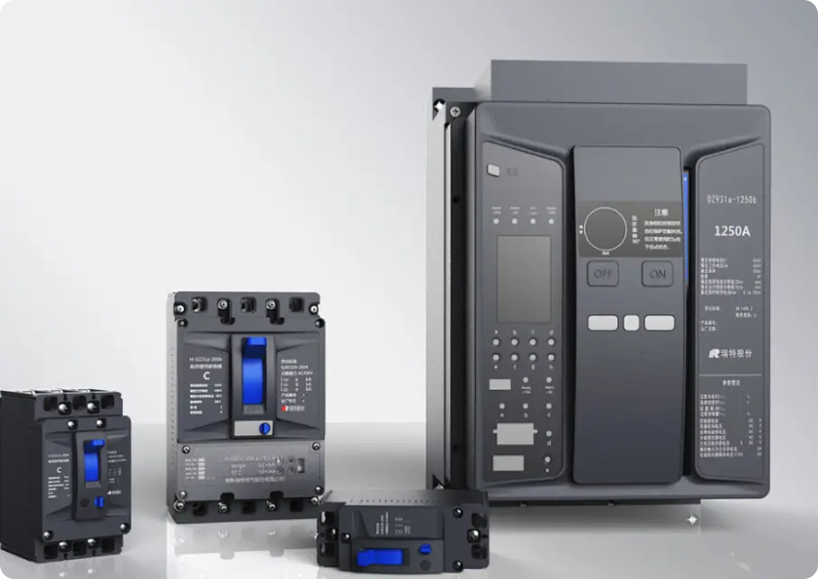
Power Systems
Power Management System, Power Supply Equipment
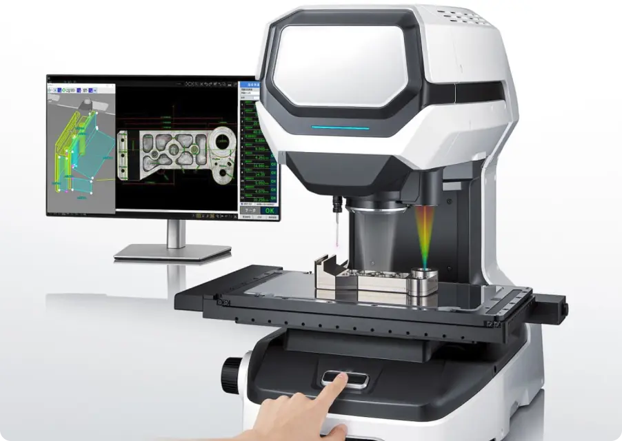
Instruments and Meters
Measuring Instrument, Testing Equipment
Why Choose EIPEKS for PCB Development?
Flexible Orders and Fast Delivery
We promise to deliver projects within the scheduled time and provide flexible ordering options. You can determine the appropriate order quantity according to your needs.

Extensive Expertise and Experience
Our project team has successfully completed hundreds of PCB development projects. Our expertise covers all aspects, from schematics and layout to packaging and BOM.

End-to-End Solutions
We provide comprehensive PCB development services, including 3D design, hardware development, software development and embedded system development to to meet all your design needs.

Integrated Manufacturing and Assembly
Our manufacturing and assembly processes are integrated, avoiding DFM and DFA non-compliance issues caused by cooperation with multiple suppliers. This integrated approach ensures a seamless connection between design and production, reducing potential delays and errors.

How We Work With You
Preliminary Assessment
To better understand your project vision and needs, we will communicate with you in depth. After signing a non-disclosure agreement, our team will assess your project, gather your requirements, analyze market competitors, and develop a preliminary strategy.
Project Plan
Once project requirements are confirmed, we'll work with you to create detailed technical specifications, budget, and schedule. Our project team will conduct a comprehensive project assessment, refine resource allocation, and ensure the smooth progress of the project.
Development Phase
During the R&D phase, we will carry out component selection, schematic design, PCB layout design, and prototype production. At the same time, our technical team will carry out firmware development, 3D modeling, and simulation testing. We will also maintain regular communication with you to report on the project progress and adapt to any new requirements or goal adjustments.
Testing and Compliance
We will conduct rigorous testing to ensure that the product is error-free and meets industry standards. All tests will be conducted under real operating conditions, including those required for product certification. If problems are found, we will make the necessary modifications to resolve them and ensure product compliance.
Manufacturing Support
As your project moves to large-scale production, we'll provide full production documentation and technical support, including a detailed Bill of Materials (BOM). If needed, we can help you choose a suitable manufacturer and ensure a smooth production process.

Preliminary Assessment
To better understand your project vision and needs, we will communicate with you in depth. After signing a non-disclosure agreement, our team will assess your project, gather your requirements, analyze market competitors, and develop a preliminary strategy.

Project Plan
Once project requirements are confirmed, we’ll work with you to create detailed technical specifications, budget, and schedule. Our project team will conduct a comprehensive project assessment, refine resource allocation, and ensure the smooth progress of the project.

Development Phase
During the R&D phase, we will carry out component selection, schematic design, PCB layout design, and prototype production. At the same time, our technical team will carry out firmware development, 3D modeling, and simulation testing. We will also maintain regular communication with you to report on the project progress and adapt to any new requirements or goal adjustments.

Testing and Compliance
We will conduct rigorous testing to ensure that the product is error-free and meets industry standards. All tests will be conducted under real operating conditions, including those required for product certification. If problems are found, we will make the necessary modifications to resolve them and ensure product compliance.
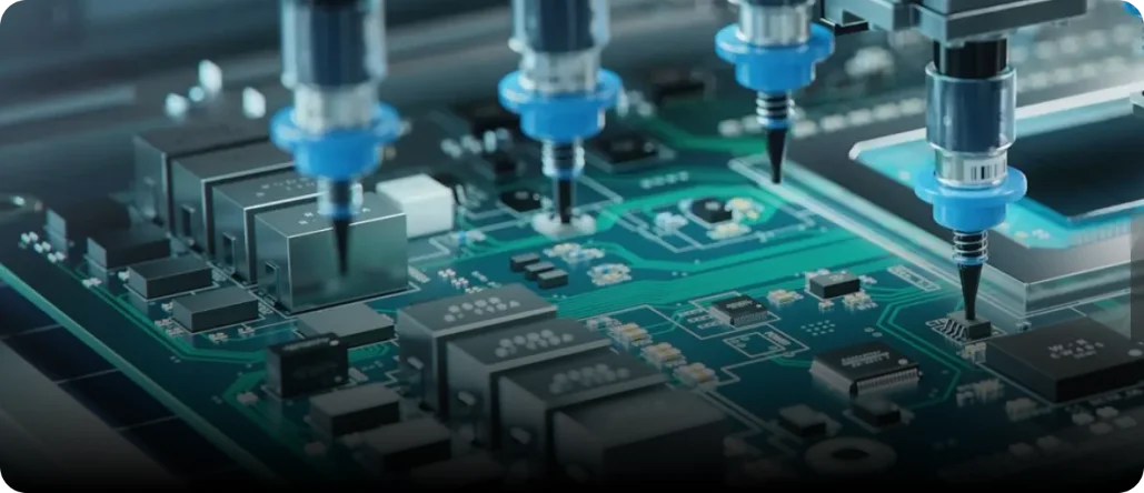
Manufacturing Support
As your project moves to large-scale production, we’ll provide full production documentation and technical support, including a detailed Bill of Materials (BOM). If needed, we can help you choose a suitable manufacturer and ensure a smooth production process.
Customer Case Showcase

Portable Home Gym
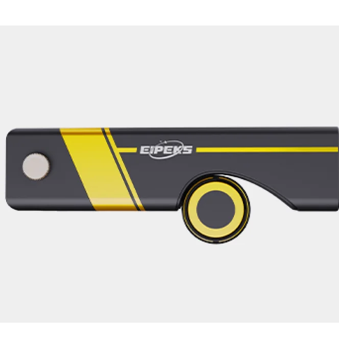
Bicycle Electrification Kit
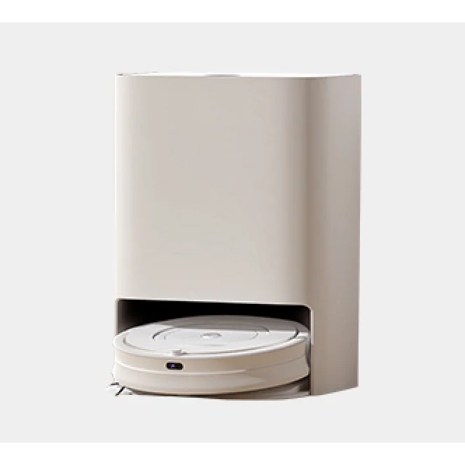
Intelligent Cleaning Robot
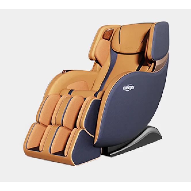
Intelligent Massage Chair
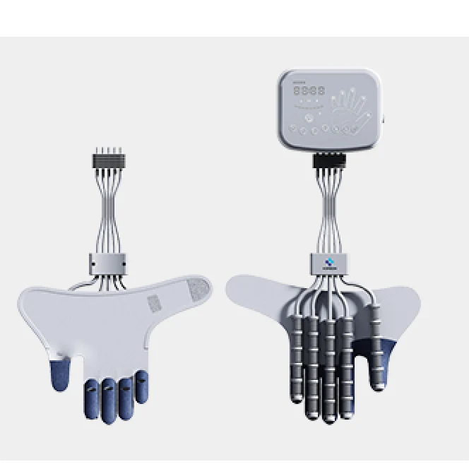
Rehabilitation Glove
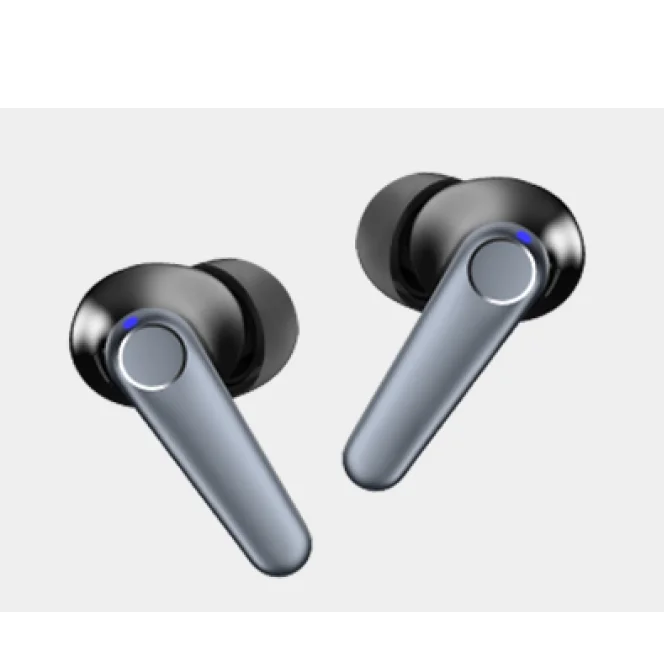
Quantum Smart Headphone
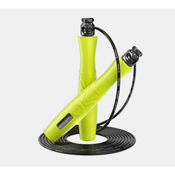
Jump Rope
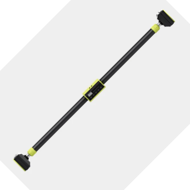
Intelligent Pull-up Bar
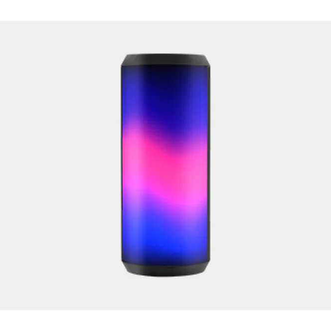
Bluetooth Speaker
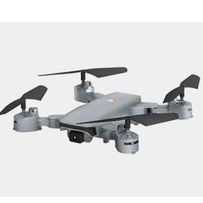
Dual-Camera Drone
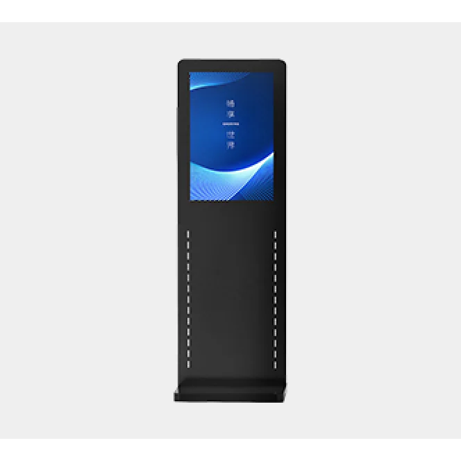
Outdoor LCD Advertising Display
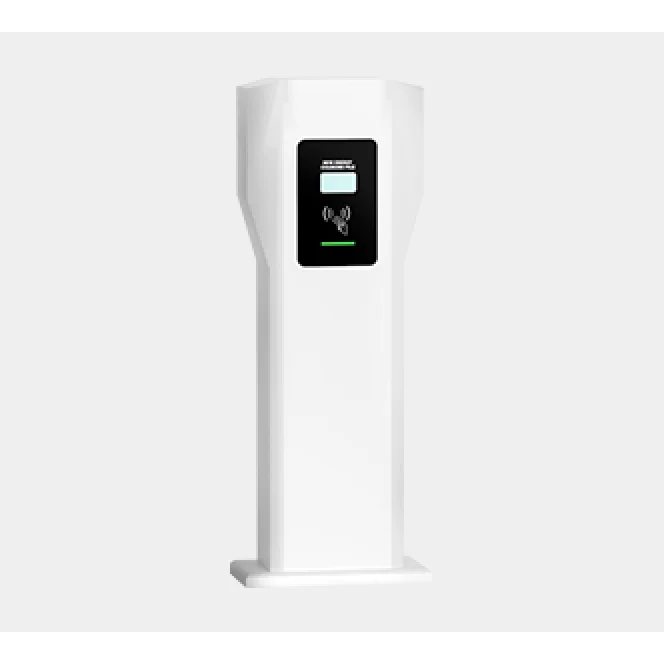
Electric Vehicle Charging Station
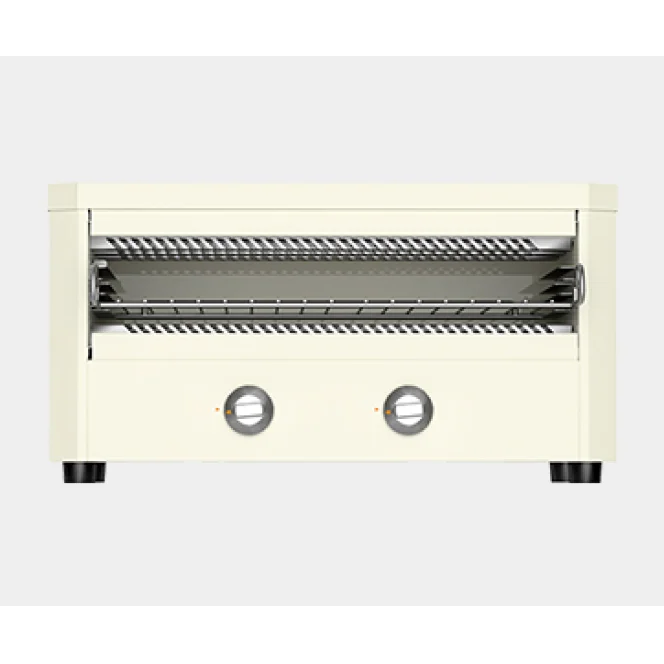
Household Electric Oven
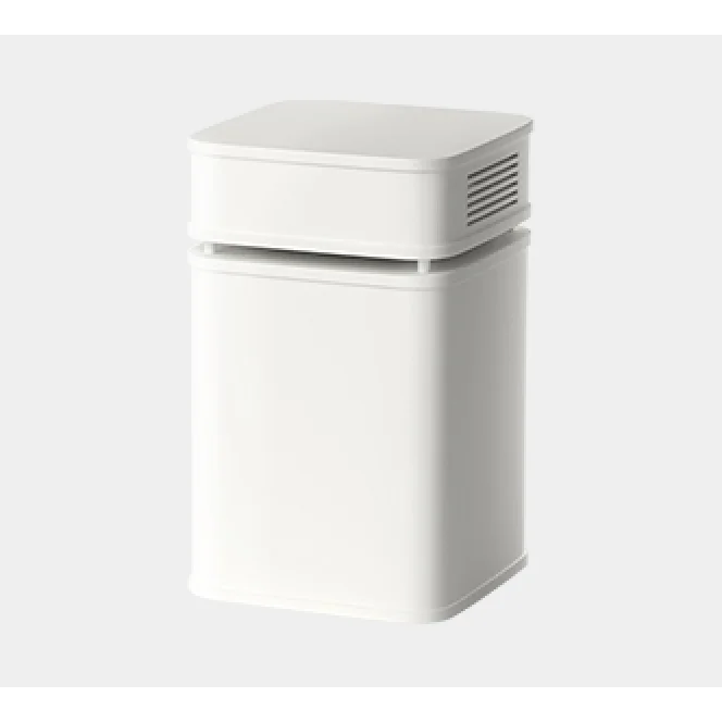
Air Purifier
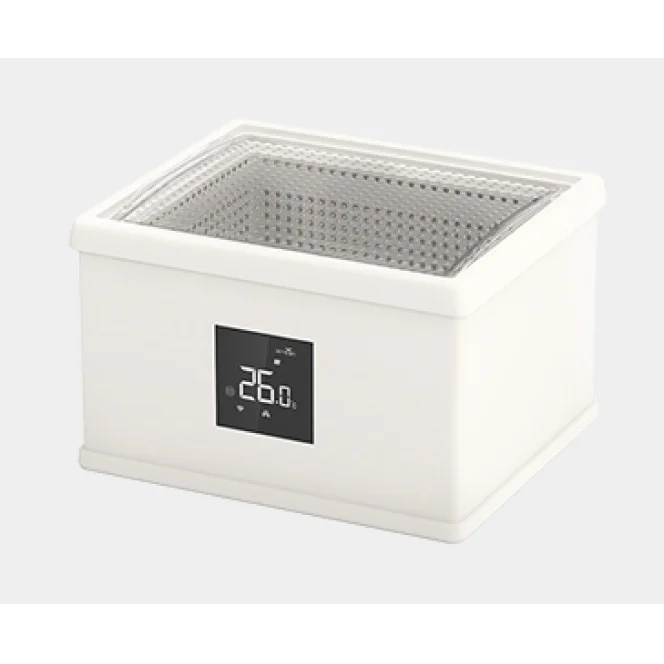
Pet Dryer Box
Trusted by Customers Worldwide for Our PCB Development Services

Contact us to get EIPEKS professional service!
Our customer service team provides 24/7 online support and is always ready to answer any questions you have about PCB development.

